Introduction
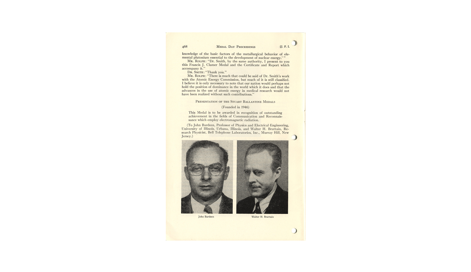
First as friends and later as lab partners, John Bardeen and Walter Brattain were the perfect complements to one another. They met in Princeton, New Jersey, and worked together to improve the field of communications.
Who were John Bardeen and Walter Brattain? What was the Point Contact Transistor, and who should be credited with its invention?
Midwestern Mentality
Walter Brattain and John Bardeen were highly educated and well-respected in the field of theoretical physics. Both scientists grew up in America's Heartland—Brattain in Washington State and Bardeen in Wisconsin. They became friends in Princeton, New Jersey, when Bardeen was working to complete his PhD in theoretical physics at Princeton University. He and Robert Brattain, Walter's brother, were classmates, and the young men bonded over their mutual enjoyment of bridge and bowling, united by their Midwestern upbringing. Brattain and Bardeen complemented each other first as friends and later as lab partners, and by all accounts enjoyed working together to improve the field of communications.
An Experimentalist and a Theorist
Walter Brattain and John Bardeen co-invented the transistor fourteen years after their initial meeting in Princeton, at which point both men were in the employ of Bell Laboratories. Brattain was good-humored and outgoing, while Bardeen was on the quieter side. Brattain was a skilled experimentalist, and had a reputation for being able to build anything in the laboratory. Bardeen was an incisive thinker capable of examining problems from a variety of angles and of generating thoughtful, ingenious solutions. Bardeen developed a reputation for answering questions at whatever level he thought the inquirer best able to understand. One of his colleagues at the Naval Ordinance Laboratory commented, "There was no intellectual snobbery about him at all."
The War Effort
World War II spurned many of the efforts into electronic and communications research in the United States. Both Bardeen and Brattain worked to further war-related research projects. Brattain worked for twenty-two months on the magnetic detection of submarines, while Bardeen devoted four years to working for the Naval Ordinance Laboratory (NOL) on numerous classified projects. Bardeen would observe in 1945, "The armed services have control of scientific talent in this country." He left the NOL to pursue research on semiconductors, indicating to his NOL colleagues that this research would ultimately benefit the U.S. in the area of communications technology, a field in which Germany and Russia were emerging as competitors. Semiconductors play a key role in radio and radar, and thus their advancement stood to sophisticate U.S. military devices.
What's the Point?
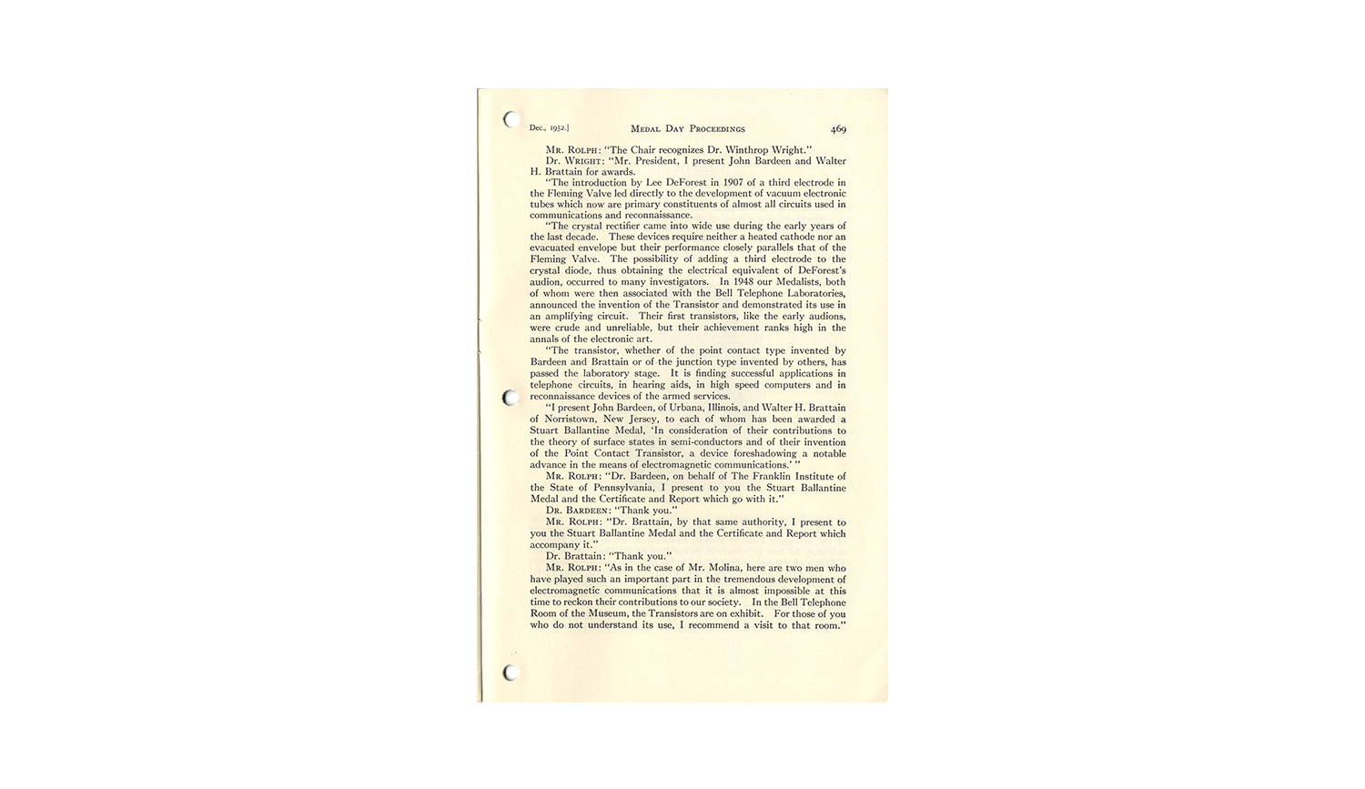
Bardeen and Brattain received accolades for their development of the first transistor. The transistor serves two primary functions: it conducts electricity in a particular direction, and it amplifies electricity. Transistors are a key component of myriad electronic devices, from hearing aids to radios to radar. The first transistor was half an inch high; today seven million transistors are able to fit snugly in a single computer chip. Though the transistor has been modified and streamlined over the years, Bardeen and Brattain laid much of the groundwork for this device with their achievement in November of 1947.
Metal Grid Makes Magic
The vacuum tube was the predecessor to the transistor. A vacuum tube is a glass tube surrounding an area from which all gases have been removed, which is known as a vacuum. In 1883, Thomas Edison discovered that a vacuum tube is able to conduct electricity when electrical contacts are attached to its end. A light bulb is an example of such a vacuum tube. In the 1900s, inventor Lee De Forest enabled the vacuum tube to meet its full potential when he invented the audion. The audion was able to conduct electricity in a particular direction, and furthermore was able to increase the electric current as it traveled. He achieved this feat by placing a metal grid in the middle of a vacuum tube. He introduced a second electric current into the vacuum tube in order to change the voltage on the grid, and was then able to control the flow of a second and more powerful current through the tube. This resulted in the emergence of a stronger current from the electrical base of the vacuum tube.
Conduction
Materials can be defined by their ability (or lack thereof) to conduct electricity. Materials are classed into one of four groups, depending on how well they conduct electricity. They can be classified as insulators, conductors, semiconductors or superconductors. Every material is composed of atoms, and every atom has a nucleus with a certain number of electrons circling it. The way these electrons are arranged around the nucleus is what determines a given material's ability to conduct electricity.
Conductors
The electrons in an atom travel around the nucleus on specific bands, or tracks. Each track can hold one specific number of electrons, and once that track is full, any electrons that are left over must proceed to the next track. Some of the tracks are closer to each other than others, and which track an electron is on determines how much energy that electron contains. The innermost track requires the least amount of energy, and in every atom, the electrons crowd as close to the nucleus as possible. Thus, the innermost track is filled first, and the outermost track is sometimes not filled. If it is not filled, it is possible for an electron from a nearby atom to jump from its track onto the unfilled track of its neighbor. This jumping of electrons creates an electrical current, and atoms with empty spaces in their outermost electron tracks are thus able to be conductors (they are able to conduct electricity).
Semiconductors
In an atom, the proximity of the next empty track to the outermost filled track determines whether or not that atom can conduct electricity. If the next empty track is close by, the electrons in the outermost track might be able to jump up to it if they are given a jolt of energy from an outside source like a flash of light. When this happens, the electron that jumps is in a track with empty spaces, enabling other electrons to jump from other atoms and join it as it travels around the nucleus. Atoms with a full outside track which is very close to the next track are thus sometimes able to conduct electricity (specifically, at times when they are given a jolt of energy), and they are thus known as semiconductors.
Insulators and Superconductors
If the next empty track in an atom is so far away that the electrons in the outermost filled track cannot jump to it even when they are given a jolt of energy, then the atom is known as an insulator. If an atom is an insulator, it is not a conductor of electricity.
Atoms known as superconductors are still being explored and experimented with. They are fascinating because their electrons achieve a kind of attraction for each other. Since electrons are negatively-charged particles, they usually repel each other. However, the ability of superconductors to attract electrons enables electrons to jump easily from one atom to the next. Superconductivity has, to date, only been achieved at very low temperatures, though scientists are in the process of discovering materials that "superconduct" closer to room temperature.
One Way
A diode, otherwise known as a "rectifier," is a device through which electricity can flow in only one direction. The earliest diodes were made of crystal and were used in home radio kits to direct radio signals. A fine wire known as a "cat's whisker" was used to feed a weak radio signal into the crystal, and the crystal then removed the high frequency radio carrier signal. This allowed the part of the signal carrying the audio information to come through, and thus signals carrying news and music could be heard.
Crystals contain impurities, making some sections more resistant to electrical flow than others. In 1939, scientist Russell Ohl discovered that it was the boundary between sections of different purity that enabled the crystal to direct electricity in one direction. Each "side" of the boundary was a semiconductor, and some semiconductors carried electricity more easily than others. After this discovery was made, diodes were constructed with two sides, separated by a boundary. One side was made up of a semiconductor that carried electrons easily, and the other side of a semiconductor that did not carry electrons easily. Electrons jumped easily from the side that did not carry electrons easily to the side that did. Electricity was thus conducted successfully in only one direction.
Golden Triangle
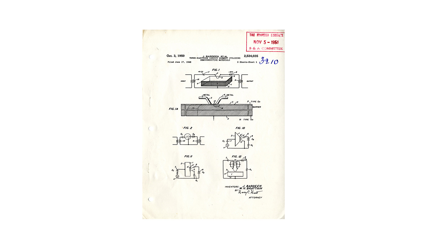
The Point Contact Transistor invented by Bardeen and Brattain contained a triangle covered in gold foil and a crystal of germanium on a spring. Brattain attached a single strip of gold foil over the point of a plastic triangle, and then used a razor blade to slice through the gold right at the tip of the triangle. When the contraption was complete, it successfully directed electrical current from one gold contact to the other, and in the process enable the current to emerge from the second gold contact stronger than it was when it entered the first.
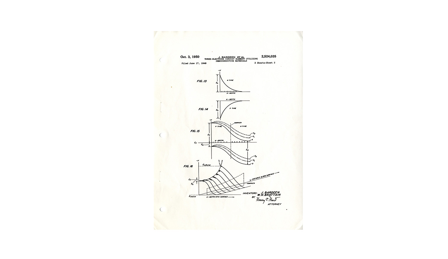
The crystal of germanium was the semiconductor present in Bardeen and Brattain's transistor. It sat on a metal plate attached to a voltage source. As a semiconductor, germanium can either let a great deal of electrical current through or none at all, depending on how it is treated. The germanium used by Bardeen and Brattain had an excess of electrons, but the scientists soon discovered that, when an electric signal traveled in through the gold foil, it injected holes (positive particles, the opposites of electrons) into the surface. This created a thin layer along the top of the germanium that contained too few electrons.
The P-N Junction and its Function
Semiconductors with too many electrons are classified as N-type, while semiconductors with too few electrons are classified as P-type. The boundary between these two types of semiconductors is known as a P-N junction, and when the P-N junction is present, current can begin to flow from one side to the other.
Punching Holes
In building their transistor and creating this junction, Bardeen and Brattian realized that, when a small current came in through one gold contact, it changed the nature of the germanium semiconductor so that a larger, separate current began flowing across the germanium and out the second current. This little current altered the flow of a much bigger current, and thus when the current emerged from the transistor, it was amplified. The "holes" punched into the semiconductor by the first current functioned in the same way as the metal grid which Lee De Forest had inserted into the vacuum tube to enable amplification earlier that century.
A semiconductor like germanium is extremely sensitive to how many extra or missing electrons it has inside. Each time the input signal punches more holes in the germanium, it changes the way current flows across the crystal. The output current varies with the input current. This sensitivity to changes in input current is what enables transistors to carry and amplify complex sounds like a human voice or an orchestra recording.
Holes in the Transistor Effect Theory
A paragraph included in a 1951 edition of "Science" states the transistor effect and the critical discovery of "holes" made by Bardeen and Brattain with the following:
"The functioning of transistors can be explained using the theory of semiconductors developed about 1931. This theory predicts that electrons in a semiconductor behave normally like negatively charged electrons and also cooperate so as to mimic the behavior of positively charged electrons, or "holes.""
A Fortunate Act of Frustration
Bardeen and Brattain moved steadily toward discovering the transistor effect after Bardeen, in frustration, threw an early model of the transistor into a thermos of water. He did so in order to eliminate the condensation that kept mysteriously building up on the surface of the germanium acting as the contraption's semiconductor. Though an impulsive move made in a moment of frustration, the immersion in water enabled Bardeen's model to amplify electricity more successfully than ever before.
From Collegial Researcher to Covert Operator
At Bell Labs, Bardeen and Brattain worked under the direction of William Shockley. Prior to working together at Bell, Bardeen and Shockley both spent in Cambridge, Massachusetts. Their time there overlapped from 1935 to 1936, while Bardeen was holding an appointment at Harvard University and Shockley was completing coursework at the Massachusetts Institute of Technology (MIT). Both men got along well, and discussed their current research. When he was working on the development of the transistor a decade later, Bardeen would draw on the knowledge of semiconductor surface states he gained from Shockley.
Despite the camaraderie Shockley enjoyed with Bardeen and other members of his Bell Labs research team, he began to withdraw from his colleagues as the Point Contact Transistor approached completion. He worked on his own in the privacy of his home, emerging with the development of the Joint Transistor shortly after Bardeen and Brattain went public with their invention. All three men were awarded the Nobel Prize in Physics in 1956 for their investigations on semiconductors and their discovery of the transistor effect.
The Shockley Controversy
The exact nature of Shockley's contributions to the development of the transistor remains a subject of controversy, as does the question of how much (if any) credit he should be given for its invention. What is clear is that Shockley's invention of the Joint Transistor and other of his subsequent achievements overshadowed the work of Bardeen and Brattain, and his name and his work hold a more prominent place in history. Shockley's treatment of Bardeen and Brattain eventually prompted both men to break away from Bell Labs, and severed any good relations between himself and his former colleagues.
Despite the differing opinions on the subject, Bardeen and Brattain are widely credited with the invention of the Point Contact Transistor, and even if their names are not as well-remembered as Shockley's, their work significantly contributed to the improvement of the field of communications.
Bending the Rules
The contents of the case file compiled on Bardeen and Brattain reveal that there was some question as to whether or not their invention of the Point Contact Transistor met the requirements for receipt of the Ballantine Award. Specifically, the Committee on Science and the Arts debated whether or not the Transistor had a direct effect on the field of communications. It was decided that, though the Point Contact Transistor was not capable of facilitating communication on its own, the device "made possible a desired end." Speaking to this point, Awards Committee Member W. R. Wright compared Bardeen and Brattain to theoreticians like Maxwell and Hertz who had received the award in the past: "In the case of theoreticians...one can point to no physical invention for which credit can be given but surely the whole field of electromagnetic invention stands on their shoulders."
Expanding the Scope
In light of this insight, the committee members worked to modify the award citation accompanying the Ballantine Medal, emphasizing the value of the Point Contact Transistor in the overall advancement of electromagnetic communication. Committee member Albert F. Murray recommended expanding the scope of the Ballantine Medal in a letter to Dr. Wright, pointing out that the Ballantine Medal "is the only S. and A. award connected with the field of radio, radar, television and the like, therefore its scope might be enlarged to cover inventions...in this dynamic domain."
Credits
The Bardeen and Brattain presentation was made possible by support from The Barra Foundation and Unisys.
Thanks to the Collections of the University of Pennsylvania Archives.

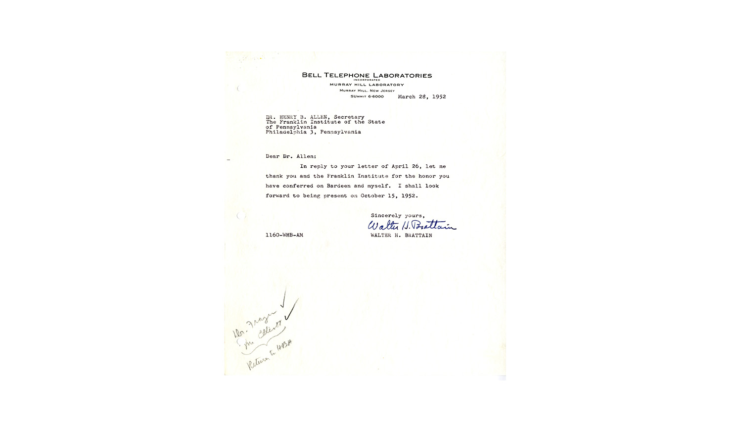


Read the Committee on Science and the Arts Report on Drs. John Bardeen and Walter Brattain and their work on semi-conductors and their invention, the Point Contact Transistor.